Sony Semiconductor Solutions to Release Advanced 1/2-type CMOS Sensor for Mobile Applications Featuring Industry’s First*1 RB2×2 OCL Pixel Structure for Both High Resolution and AF Performance
New pixel design and algorithm deliver more than 20% higher definition compared to Sony’s conventional product
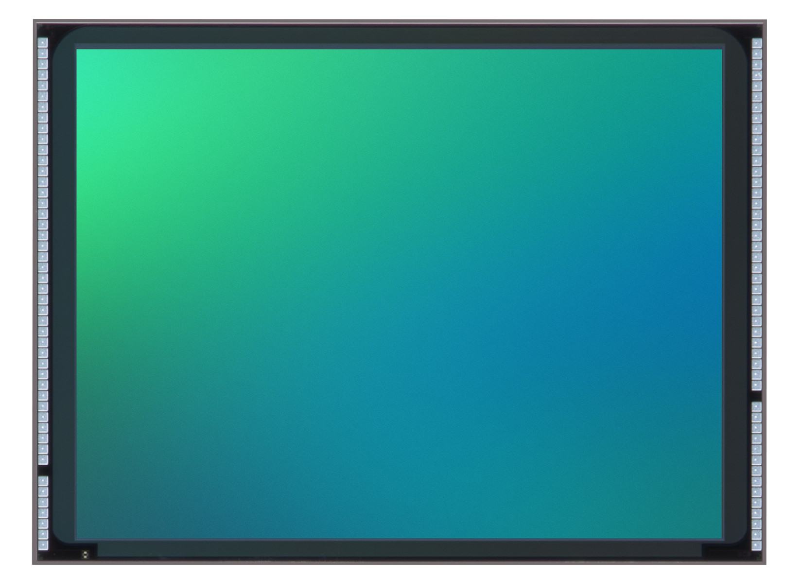
Sony Semiconductor Solutions Corporation (Sony) today announced the upcoming release of the LYTIA 610, a 1/2-type approximately 64-effective megapixel CMOS image sensor with the RB2×2 On Chip Lens (OCL) pixel structure. This is the industry’s first*1 product with this pixel structure to be mass produced.
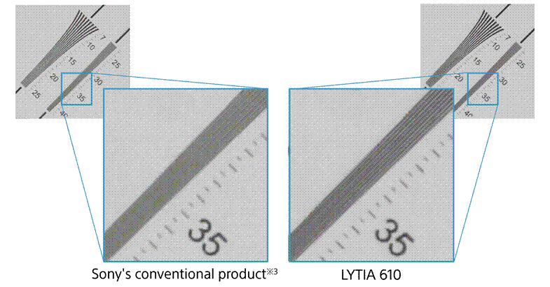
By combining the RB2×2 OCL pixel structure with dedicated array conversion processing (remosaicing) optimised for this structure, the new product achieves both improved resolution and excellent autofocusing (AF) performance at the same time. It offers more than 20% improvement in spatial resolution*2 compared to Sony’s conventional product with the same pixel size,*3 allowing telephoto cameras to capture subjects with fine detail.
The improved readout speed also enables 4K 120 fps video recording for the first time on Sony’s 1/2-type sensor. This reduces the performance gap with the large sensors used on main cameras and suppresses variations in image quality across multi-lens camera systems, enabling a more uniform shooting experience.
*1 Among CMOS image sensors. According to Sony’s research (as of announcement on June 24, 2026).
*2 Spatial resolution: An indicator used for evaluating image definition. This figure quantifies the level of detail at which thin, alternate black and white lines can be clearly distinguished. A higher value indicates a finer depiction of detail in the subject.
*3 Compared with the LYTIA 601 mobile CMOS image sensor with a 2×2 OCL construction and pixel size of 0.7 µm.
Model name | Mass-production shipment date |
LYTIA 610 1/2-type 64-effective-megapixel*4 stacked CMOS image sensor for mobile applications | End of June 2026 |
*4 Based on the image sensor effective pixel specification method.
Main Features
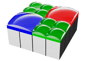
■ High resolution and AF performance achieved through the industry’s first*1 RB2×2 OCL pixel structure and dedicated algorithm
The RB2×2 OCL pixel structure features an optimal arrangement of a 1×1 OCL structure for ensuring high resolution and a 2×2 OCL structure for enhancing AF performance on a single sensor.
Sony’s technology for designing an optimal balance of lenses with different sizes and curvatures on a single surface, together with its high-precision manufacturing technologies, has enabled the coexistence of two types of OCL structures within a Quad Bayer array sensor. Specifically, G (green) pixels, which contribute to better image definition, utilize the 1×1 OCL structure with superior resolution performance. The 2×2 OCL structure, where four pixels share a single lens, is used on R (red) and B (blue) pixels to serve as phase difference detection pixels.
Furthermore, a new dedicated remosaicing (array conversion) processing algorithm was developed to further enhance the imaging performance of this unique pixel array. The optimized pixel structure and signal processing together deliver more than 20% improvement in spatial resolution compared to the conventional product*3 of the same pixel size, while maintaining superb AF performance.
■ Sony’s first 1/2-type sensor to support 4K 120 fps video recording
The logic circuits on this product employ fine processing for low energy consumption. Additionally, the AD converter (analog-to-digital conversion circuit) has been optimised through increased parallelisation to achieve high-speed data readout that is double that of the conventional 1/2-type sensor.*3
The improved readout speed enables 4K 120 fps video recording for the first time on Sony’s sensor of the same size, which had been difficult to achieve with previous designs. This design makes it possible to record smooth videos of fast-moving subjects and superior-quality slow-motion videos. It also supports 4K 60 fps HDR video recording, which is ideal for capturing high-contrast scenes.
These improvements in video performance reduce differences in image quality and appearance when switching between main and sub cameras, enabling smooth transitions across multi-lens camera systems for seamless video shooting experiences.
Related Link
For Slow-motion Sample (4K 120 fps), please visit our website:
https://www.sony-semicon.com/en/news/2026/2026062401.html
For more information on LYTIA, the Sony’s mobile image sensor brand, please visit the LYTIA brand site:
https://www.sony-semicon.com/en/products/is/mobile/index.html
Key Specifications
Model name |
| LYTIA 610 |
|---|---|---|
Image size |
| 1/2.0-type (diagonal 8.095 mm) |
Effective pixels |
| Approx. 64 megapixels |
Unit cell size |
| 0.7 µm × 0.7 µm (H × V) |
Color filter |
| Quad Bayer Coding |
OCL pattern |
| RB2×2 OCL |
Frame rate | 64 megapixels (4:3) | 24 fps |
| 16 megapixels (4:3) | 60 fps 30 fps (DAG-HDR) |
| 4K2K (16:9) | 120 fps 60 fps (DAG-HDR) |
Power supply | Analog | 2.8 V/1.8 V |
| Digital | 0.81 V |
| Interface | 1.8 V or 1.2 V |
Output interface |
| MIPI® C-PHY 2/3 trio, Max. 4.5Gsps/trio MIPI D-PHY 2/4 lane, Max. 2.5Gbps/lane |
* LYTIA and the LYTIA logo are registered trademarks or trademarks of Sony Group Corporation.
* All product and service names that appear in this announcement are the trademarks or registered trademarks of their respective owners.
Media inquiries
Public Relations, Sony Semiconductor Solutions Corporation: semicon.press@sony.com
About Sony Semiconductor Solutions
Sony Semiconductor Solutions Corporation is a wholly owned subsidiary of Sony Group Corporation and operates across the extensive fields of the semiconductor device business, centered primarily on image sensors, a field for which it has maintained the global number one position. We strive to provide advanced imaging technologies that bring greater convenience and joy to people’s lives. In addition, we are committed to developing and bringing to market new kinds of sensing technologies with the aim of offering various solutions that will take the visual and recognition capabilities of both humans and devices to greater heights.
Visit us at: https://www.sony-semicon.com/en/index.html